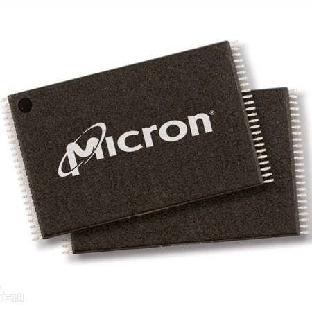
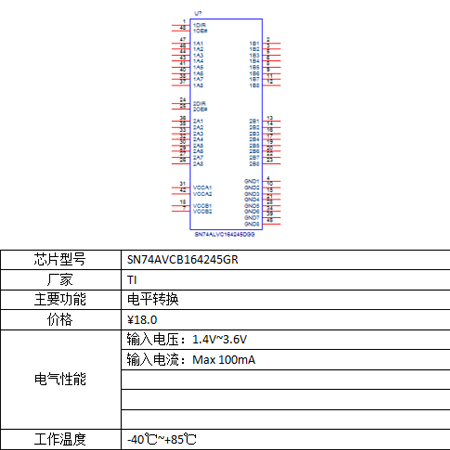
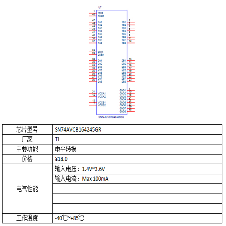
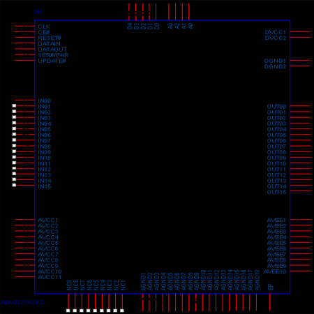
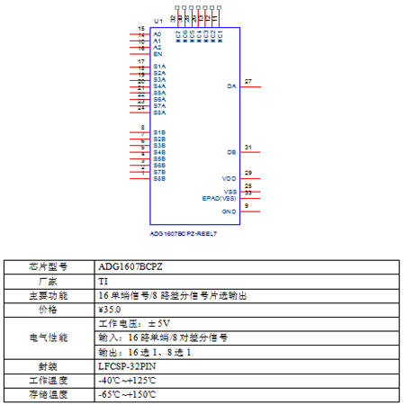
芯片型号 | AS3722-BCTT-T1V2-09/10 |
厂家 | AMS(奥地利微电子) |
主要功能 | 电源管理控制(Multi-Phase DCDC controller PMIC) |
价格 | ¥43.00 |
电气性能 | 接口电平:2.7~5.5V; |
外接控制DCDC芯片:AS3728; | |
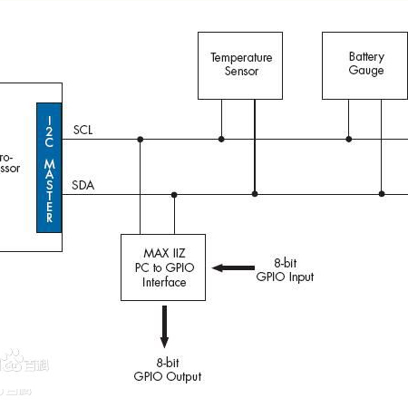
控制接口:I2C/SPI接口; | |
电源输出:11路LDO输出,4路DCDC输出和4路DCDC控制; | |
工作温度 | -40°C~+85°C |
储存温度 | -55°C~+125°C |
主要功能 | 电源管理控制; |
电气性能 | 主芯片工作电压:2.7~5.5V |
控制接口:I2C/SPI | |
输出控制:11路LDO输出,4路DCDC输出和4路DCDC控制; | |
系统工作温度 | -40°C~+85°C |
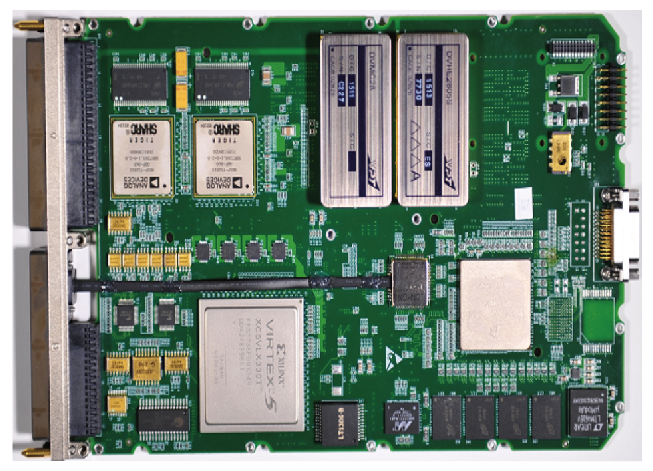
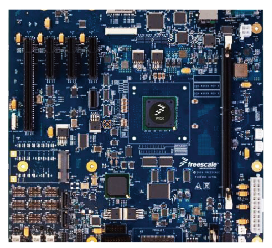
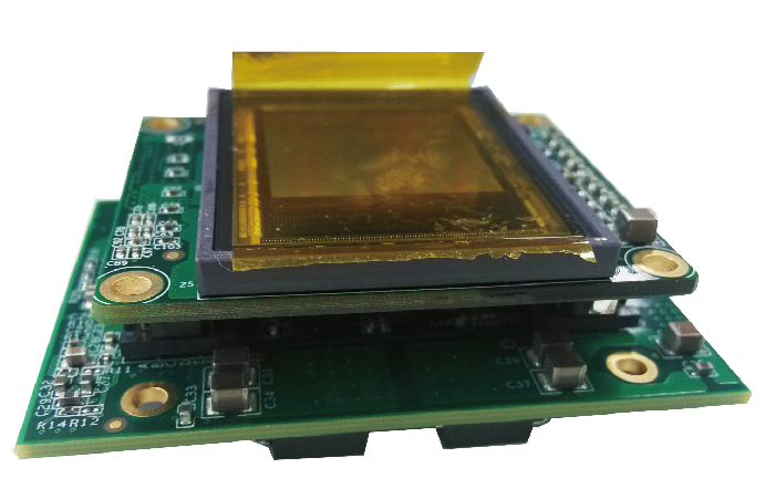
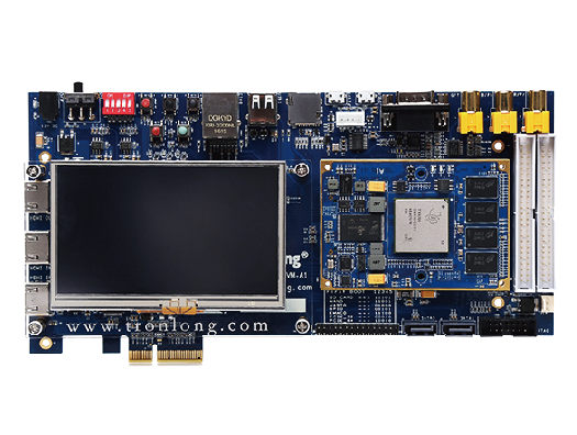
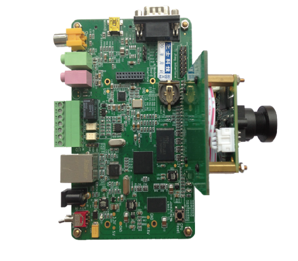
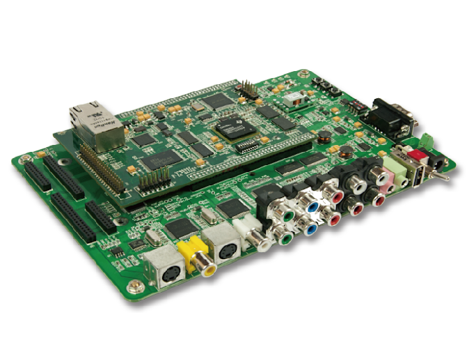
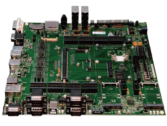
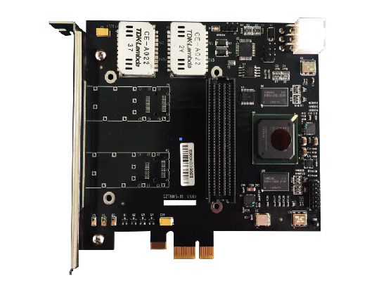
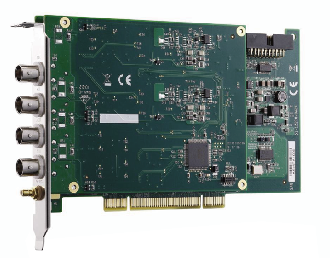
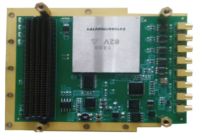
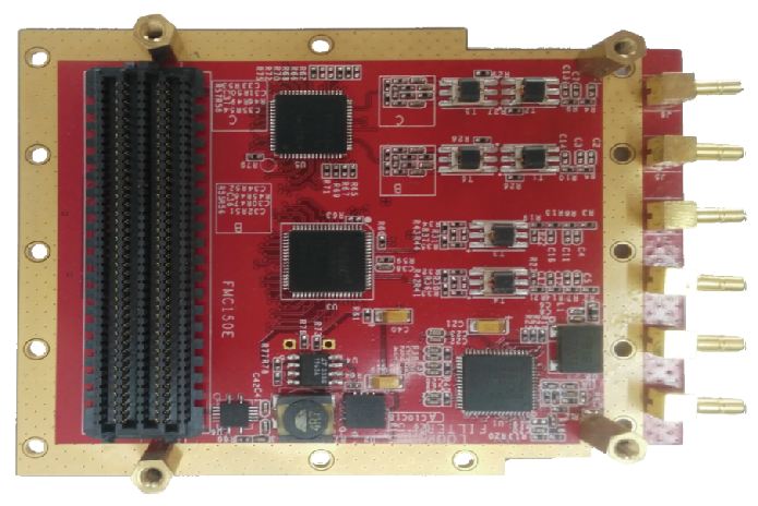
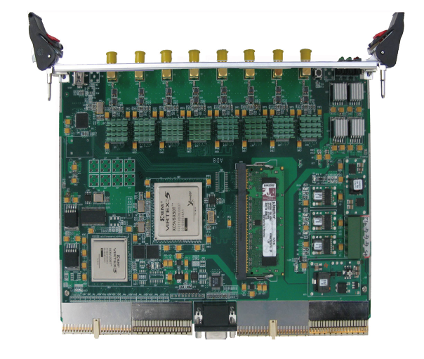
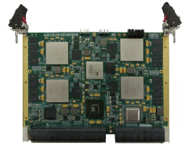
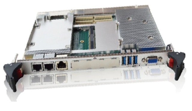
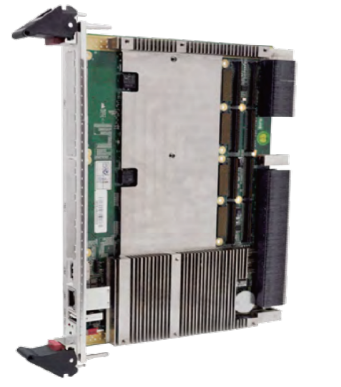
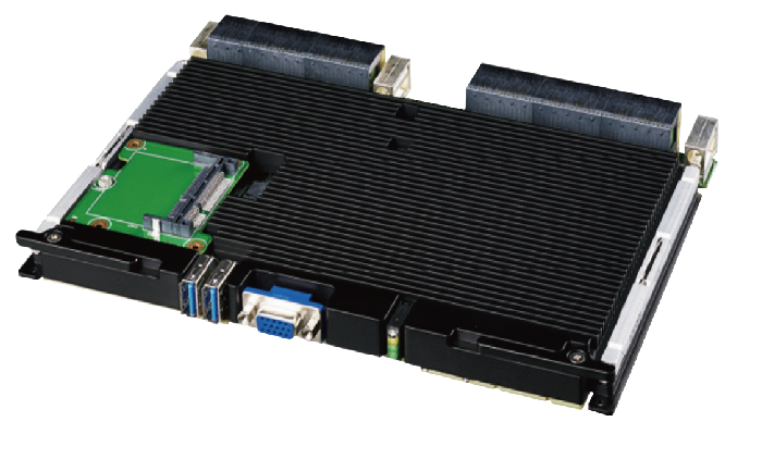
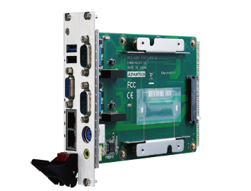
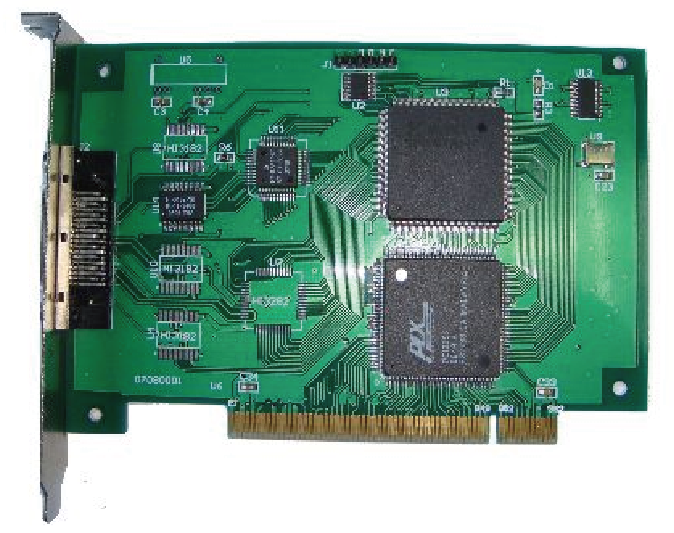
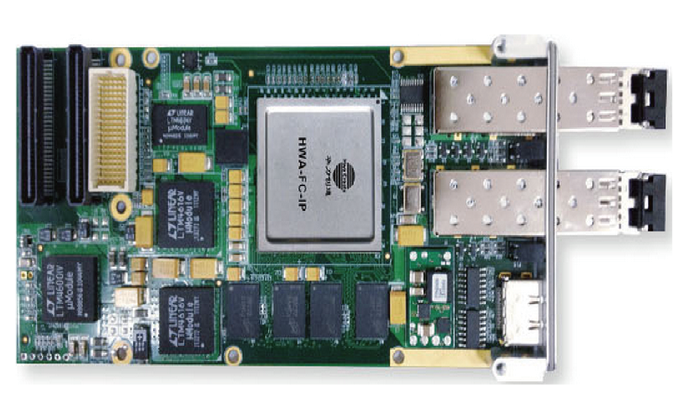
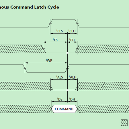
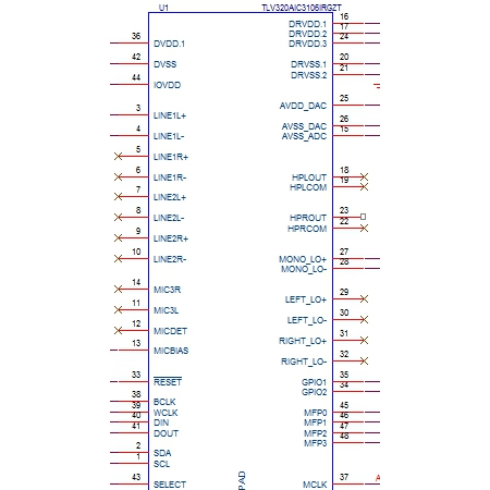
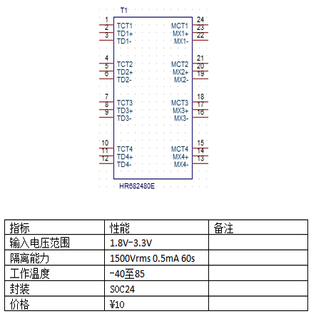
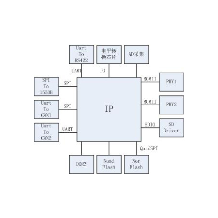
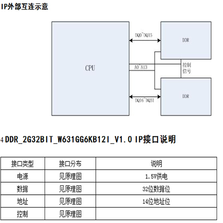
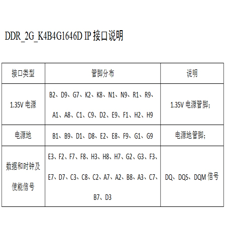
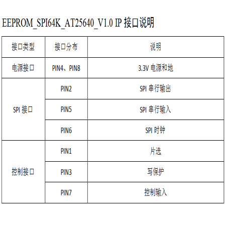
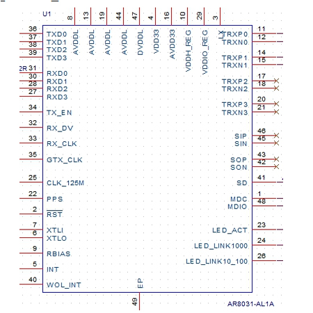
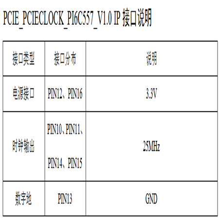
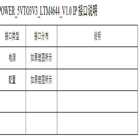
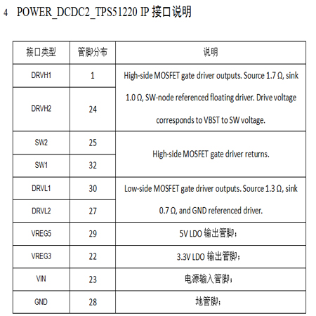
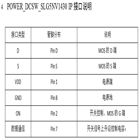
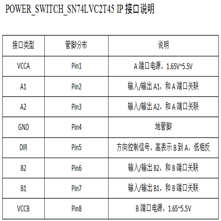
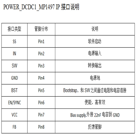
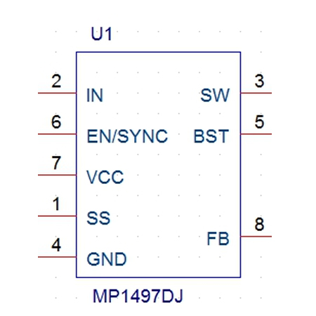
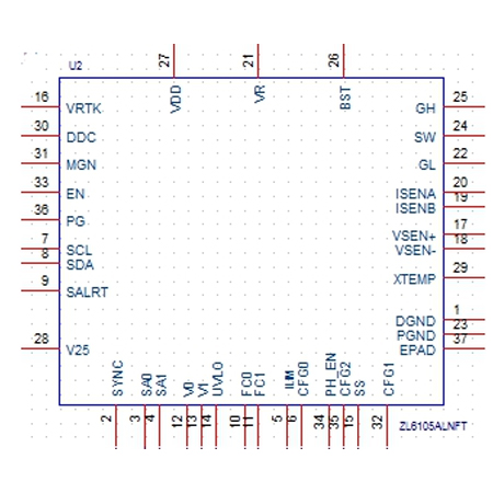
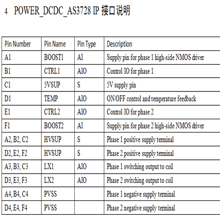
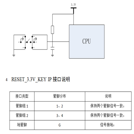
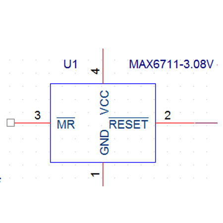
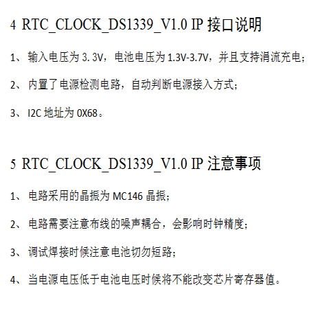
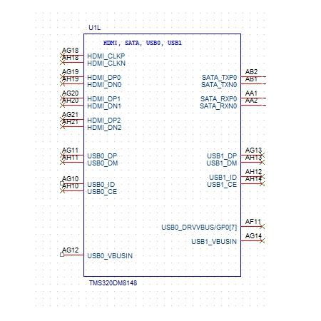
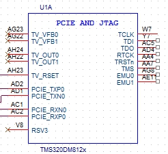
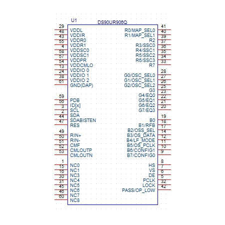
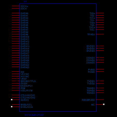
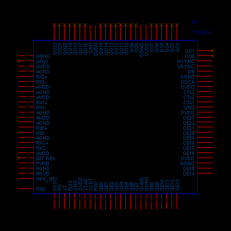
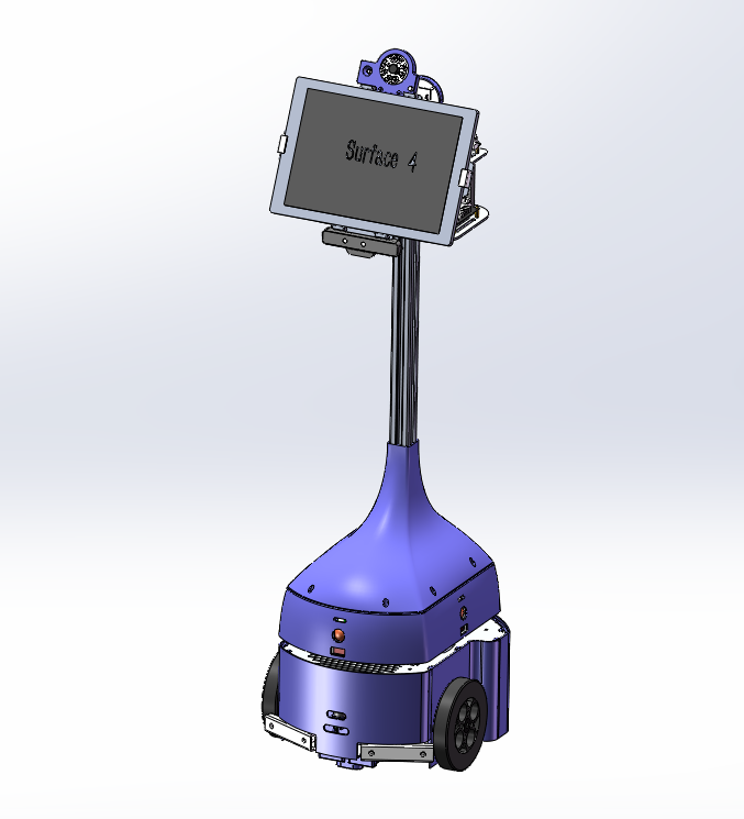
见示意图

Pin Number | Pin Name | I/O | Desc | Maximum Voltage | If not used |
F4 | SDA_SDI | DI | SPI digital input in SPI mode ;Data IO in I2C mode. | VSUP | Open |
G4 | SCL_SCLK | DI | SPI clock input in SPI mode ;SCK input in I2C mode. | VSUP | Open |
E2 | ENABLE3_SDO | DIO | SPI digital output in SPI mode | VSUP | Open |
H6 | SCSB | DI | SPI chip-select in SPI mode ;connect to VSS in I2C mode. | VSUP | VSS |
B14 | VIN_LDO0 | S | Supply pad for LDOs | 5.5V | Mandatory |
A8 | VIN_LDO1_6 | S | Supply pad for LDOs | 5.5V | Mandatory |
A6 | VIN_LDO9_10 | S | Supply pad for LDOs | 5.5V | Mandatory |
A3 | VIN_LDO3_4 | S | Supply pad for LDOs | 5.5V | Mandatory |
A12 | VIN_LDO2_5_7 | S | Supply pad for LDOs | 5.5V | Mandatory |
A4 | VIN_LDO3_SW | S | Supply pad for LDO3 switch function | 3.6V | Mandatory |
B1 | VIN_LDO11 | S | Supply pad for LDOs | 5.5V | Mandatory |
A13 | LDO0 | AO | Output voltage of LDO -NMOS_0.6 | VIN_LDO0 | Open |
B9 | LDO1 | AO | Output voltage of LDO -PMOS_1 | VIN_LDO1_6 | Open |
A9 | LDO2 | AO | Output voltage of LDO -PMOS_1 | VIN_LDO2_5_7 | Open |
B6 | VIN_LDO3_LV | S | Supply pad for LDO3 NMOS function | 3.6V | Open |
A2 | LDO4 | AO | Output voltage of LDO -PMOS_0.6 | VIN_LDO3_4 | Open |
A10 | LDO5 | AO | Output voltage of LDO -PMOS_0.6 | VIN_LDO2_5_7 | Open |
A7 | LDO6 | AO | Output voltage of LDO -PMOS_0.6 | VIN_LDO1_6 | Open |
A11 | LDO7 | AO | Output voltage of LDO -PMOS_0.6 | VIN_LDO2_5_7 | Open |
B7 | LDO3 | AO | Output voltage of LDO -PMOS_1 | VIN_LDO8 | Open |
A5 | LDO9 | AO | Output voltage of LDO -PMOS_1 | VIN_LDO9_10 | Open |
B8 | LDO10 | AO | Output voltage of LDO -PMOS_1 | VIN_LDO9_10 | Open |
B5 | LDO11 | AO | Output voltage of LDO -PMOS_1 | VIN_LDO11 | Open |
B10 | ONKEY | DI | Input pin to startup (nopullup/pull down) | 5.5V | Define level |
F8 | ENABLE1 | DI | Input pin for transition intoand out of deep-sleep mode | VSUP | Define level |
E11 | ENABLE2 | DI | Input pin for control ofDCDC0 | VSUP | Define level |
D8 | THERM | DI | Input pin for thermal event | 5.5V | Define level |
J8 | XRES_IN | DI | Input pin for reset during active state | VSUP | Define level |
L5 | XRES_OUT | DO | Push pull to VDD_GPIO_lv | VSUP | Open |
L8 | AC_OK | DI | Pin to indicate, that the AC adaptor is present | 5.5V | Define level |
D7 | LID | DI | Input pin to indicates LID status of Device | 5.5V | Define level |
C1 | XINT | DO | Push-Pull or open drain output for interrupt detection | VSUP | Open |
L9 | VSUP_GPIO | S | Supply pin for GPIOs (connect to other VSUP pins) | 5.5V | Mandatory |
F2 | VDD_GPIO_lv | S | Supply pin for GPIOs (connect to typical 1.8V or 3.3) | VSUP | Mandatory |
F1 | VSUP_GPIO | AIO | Analog GND input | - | Mandatory |
D6 | GPIO0 | DIO | General purpose input/output pin | VSUP | Open |
G6 | GPIO1 | DIO | General purpose input/output pin | VSUP | Open |
D5 | GPIO2 | DIO | General purpose input/output pin | VSUP | Open |
E4 | GPIO3 | DIO | General purpose input/output pin | VSUP | Open |
B3 | GPIO4 | DIO | General purpose input/output pin | VSUP | Open |
C2 | GPIO5 | DIO | General purpose input/output pin | VSUP | Open |
B4 | GPIO6 | DIO | General purpose input/output pin | VSUP | Open |
D2 | GPIO7 | DIO | General purpose input/output pin | VSUP | Open |
H2 | V2_5 | AO | Output voltage of low power LDO V2_5 | 3.6V | Mandatory |
J4 | CREF | AIO | Bypass capacitor for the | V2_5 | Mandatory |
J2 | RBIAS | AIO | External resistor; always connect a resistor of 220kΩ(±1%) to VSSA | V2_5 | Mandatory |
H4 | VBAT_BKUP | AIO | Backup battery input | 3.6V | Open |
A1 | VSSA | AIO | Analog GND input | - | Mandatory |
A14 | VSSA | AIO | Analog GND input | - | Mandatory |
J7 | VSSA | AIO | Analog GND input | - | Mandatory |
P1 | VSSA | AIO | Analog GND input | - | Mandatory |
P14 | VSSA | AIO | Analog GND input | - | Mandatory |
F7 | VSSA | AIO | Analog GND input | - | Mandatory |
D1 | CLK32K | DO | 32kHz clk output push/pull to VDD_GPIO_lv | VSUP | Open |
G1 | XIN32K | AIO | Connect to 32kHz crystal oscillator | V2_5 | Open |
G2 | XOUT32K | AIO | Connect to 32kHz crystal oscillator | V2_5 | Open |
K4 | GNDSENSE | AIO | Analog sense GND input(connect to VSSA on CSP) | - | Mandatory |
E1 | OC_PG | DO | Digital Output open drain to indicate over-current/power_good | VSUP | Open |
H1 | VSUP_ANA | S | System supply voltage input(connect to other VSUP pins) | 5.5V | Mandatory |
N6 | VSUP_SD2 | S | System supply voltage input of Stepdown2 (connect to other VSUP pins) | 5.5V | Mandatory |
P6 | VSUP_SD2 | S | System supply voltage input of Stepdown2(connect to other VSUP pins) | 5.5V | Mandatory |
N5 | LX_SD2 | AIO | LX node of Stepdown2 | VSUP | Open |
N7 | LX_SD2 | AIO | LX node of Stepdown2 | VSUP | Open |
P5 | LX_SD2 | AIO | LX node of Stepdown2 | VSUP | Open |
P7 | LX_SD2 | AIO | LX node of Stepdown2 | VSUP | Open |
N4 | VSS_SD2 | AIO | Power GND pin of Stepdown2 | - | Mandatory |
N8 | VSS_SD2 | AIO | Power GND pin of Stepdown2 | - | Mandatory |
P4 | VSS_SD2 | AIO | Power GND pin of Stepdown2 | - | Mandatory |
P8 | VSS_SD2 | AIO | Power GND pin of Stepdown2 | - | Mandatory |
K1 | FB_SD2 | AIO | Analog Feedback pin of SD2 | 3.6V | Open |
L1 | VSUP_SD3 | S | System supply voltage input of Stepdown3 (connect to other VSUP pins) | 5.5V | Mandatory |
L2 | VSUP_SD3 | S | System supply voltage input of Stepdown3 (connect to other VSUP pins) | 5.5V | Mandatory |
M1 | LX_SD3 | AIO | LX node of Stepdown3 | VSUP | Open |
M2 | LX_SD3 | AIO | LX node of Stepdown3 | VSUP | Open |
N1 | LX_SD3 | AIO | LX node of Stepdown3 | VSUP | Open |
N3 | VSS_SD3 | AIO | Power GND pin of Stepdown3 | - | Mandatory |
P2 | VSS_SD3 | AIO | Power GND pin of Stepdown3 | - | Mandatory |
P3 | VSS_SD3 | AIO | Power GND pin of Stepdown3 | - | Mandatory |
K2 | FB_SD3 | AIO | Analog Feedback pin of SD3 | 3.6V | Open |
N12 | VSUP_SD4 | S | System supply voltage input of Stepdown4(connect to other VSUP pins) | 5.5V | Mandatory |
P12 | VSUP_SD4 | S | System supply voltage input of Stepdown4(connect to other VSUP pins) | 5.5V | Mandatory |
L10 | FB_SD4 | AIO | Analog Feedback pin of SD4 | 3.6V | Open |
N14 | LX_SD4 | AIO | LX node of Stepdown4 | VSUP | Open |
P13 | LX_SD4 | AIO | LX node of Stepdown4 | VSUP | Open |
M13 | VSS_SD4 | AIO | Power GND pin of Stepdown4 | - | Mandatory |
M14 | VSS_SD4 | AIO | Power GND pin of Stepdown4 | - | Mandatory |
N11 | VSUP_SD5 | S | System supply voltage input of Stepdown5(connect to other VSUP pins) | 5.5V | Mandatory |
P11 | VSUP_SD5 | S | System supply voltage input of Stepdown5(connect to other VSUP pins) | 5.5V | Mandatory |
J1 | FB_SD5 | AIO | Analog Feedback pin of SD5 | 3.6V | Open |
N10 | LX_SD5 | AIO | LX node of Stepdown5 | VSUP | Open |
P10 | LX_SD5 | AIO | LX node of Stepdown5 | VSUP | Open |
P9 | VSS_SD5 | AIO | Power GND pin of Stepdown5 | - | Mandatory |
N9 | VSS_SD5 | AIO | Power GND pin of Stepdown5 | - | Mandatory |
H11 | FB_SD0_P | AIO | Positive Feedback of SD0 | 3.6V | Open |
J11 | FB_SD0_N | AIO | Negative Feedback of SD0 | 3.6V | Open |
E13 | CTRL1_SD0 | AIO | Bidirectional control pin of SD0, phase 1 | VSUP | Open |
E14 | CTRL2_SD0 | AIO | Bidirectional control pin of SD0, phase 2 | VSUP | Open |
F13 | CTRL3_SD0 | AIO | Bidirectional control pin ofSD0, phase 3 | VSUP | Open |
F14 | CTRL4_SD0 | AIO | Bidirectional control pin of SD0, phase 4 | VSUP | Open |
G13 | CTRL5_SD0 | AIO | Bidirectional control pin of SD0, phase 5 | VSUP | Open |
G14 | CTRL6_SD0 | AIO | Bidirectional control pin of SD0, phase 6 | VSUP | Open |
H13 | CTRL7_SD0 | AIO | Bidirectional control pin of SD0, phase 7 | VSUP | Open |
H14 | CTRL8_SD0 | AIO | Bidirectional control pin of SD0, phase 8 | VSUP | Open |
J14 | TEMP1_SD0 | AIO | Temperature control pin of subdie1 for SD0 | VSUP | Open |
J13 | TEMP2_SD0 | AIO | Temperature control pin of subdie2 for SD0 | VSUP | Open |
K13 | TEMP3_SD0 | AIO | Temperature control pin of subdie3 for SD0 | VSUP | Open |
K11 | TEMP4_SD0 | AIO | Temperature control pin of subdie4 for SD0 | VSUP | Open |
G9 | FB_SD1_P | AIO | Positive Feedback of SD1 | 3.6V | Open |
H9 | FB_SD1_N | AIO | Negative Feedback of SD1 | 3.6V | Open |
D13 | CTRL1_SD1 | AIO | Bidirectional control pin of SD1, phase 1 | VSUP | Open |
D14 | CTRL2_SD1 | AIO | Bidirectional control pin of SD1, phase 2 | VSUP | Open |
K14 | TEMP_SD1 | AIO | Temperature control psubdie1 for SD1 | VSUP | Open |
F11 | FB_SD6_P | AIO | Positive Feedback of SD6 | 3.6V | Open |
G11 | FB_SD6_N | AIO | Negative Feedback of SD6 | 3.6V | Open |
C13 | CTRL1_SD6 | AIO | Bidirectional control pin of SD6, phase 1 | VSUP | Open |
C14 | CTRL2_SD6 | AIO | Bidirectional control pin of SD6, phase 2 | VSUP | Open |
L14 | TEMP1_SD6 | AIO | Temperature control pin of subdie1 for SD6 | VSUP | Open |
L13 | TEMP2_SD6 | AIO | Temperature control pin of subdie2 for SD6 | VSUP | Open |
D9 | PWM_CLK1 | DI | PWM input pin for DVM control of SD0 | VSUP | Define lev |
D10 | PWM_DAT1 | DI | PWM input pin for DVM control of SD0 | VSUP | Define lev |
B11 | PWM_CLK2_ADC1 | DI | PWM input pin for DVM control of SD6 or ADC input pin | VSUP | Define lev |
B12 | PWM_DAT2_ADC2 | DI | PWM input pin for DVM control of SD6 or ADC input pin | VSUP | Define lev |
L7 | VBAT | S | High Voltage Supply pin for RTC, and voltage detection | 30V | Connect to VSUP |
L6 | EN5V | DO | Enable pin for external 5V HV stepdown to supply VSUP rails | V2_5 | Open |
1、芯片应用时,注意各路电压的输出,在没有程序驱动的情况下,默认只有4路输出;
2、该芯片的DC控制功能是需要和AS3728或者AS3729等进行配合应用的;
好评率:100%
好评数量:0个
工作速度:5分
工作质量:5分
工作态度:5分

暂无评价
CPU/GPU ¥12000.00
CPU/GPU ¥25000.00
CPU/GPU ¥10000.00
CPU/GPU ¥30000.00
CPU/GPU ¥10000.00
CPU/GPU ¥15000.00
CPU/GPU ¥10000.00
CPU/GPU ¥10000.00
其他 ¥5000.00

其他 ¥5000.00
其他 ¥10000.00
其他 ¥10000.00
其他 ¥10000.00
其他 ¥10000.00
其他 ¥10000.00
其他 ¥10000.00
FPGA电路 ¥10000.00
DSP电路 ¥10000.00
DSP电路 ¥10000.00
DSP电路 ¥10000.00
DSP电路 ¥10000.00
DSP电路 ¥10000.00
DSP电路 ¥10000.00
DSP电路 ¥10000.00
DSP电路 ¥10000.00
DSP电路 ¥10000.00
DSP电路 ¥10000.00
CPU/GPU ¥10000.00
FPGA电路 ¥10000.00
DSP电路 ¥10000.00
DSP电路 ¥10000.00
FPGA电路 ¥10000.00
DSP电路 ¥10000.00
CPU/GPU ¥10000.00
DSP电路 ¥10000.00
DSP电路 ¥10000.00
DSP电路 ¥10000.00
DSP电路 ¥10000.00
DSP电路 ¥10000.00
CPU/GPU ¥10000.00

FPGA电路 ¥10000.00
FPGA电路 ¥10000.00
模拟电路 ¥10000.00
模拟电路 ¥5000.00
模拟电路 ¥5000.00

模拟电路 ¥5000.00
模拟电路 ¥10000.00
模拟电路 ¥10000.00
DSP电路 ¥10000.00
DSP电路 ¥10000.00

DSP电路 ¥10000.00
FPGA电路 ¥10000.00

DSP电路 ¥10000.00

DSP电路 ¥10000.00
DSP电路 ¥10000.00
DSP电路 ¥10000.00
CPU/GPU ¥20000.00
CPU/GPU ¥20000.00
CPU/GPU ¥20000.00
CPU/GPU ¥20000.00
CPU/GPU ¥15000.00
CPU/GPU ¥20000.00
CPU/GPU ¥18000.00
CPU/GPU ¥20000.00
其他 ¥10000.00
其他 ¥6000.00
其他 ¥2000.00
其他 ¥3000.00
其他 ¥12000.00
其他 ¥8000.00
FPGA电路 ¥5000.00

MCU电路 ¥4800.00
嵌入式 ¥50000.00

嵌入式 ¥50000.00

嵌入式 ¥50000.00
嵌入式 ¥50000.00

嵌入式 ¥50000.00
嵌入式 ¥50000.00

嵌入式 ¥50000.00
嵌入式 ¥50000.00
嵌入式 ¥50000.00

嵌入式 ¥50000.00

嵌入式 ¥50000.00
嵌入式 ¥50000.00
嵌入式 ¥50000.00
嵌入式 ¥50000.00

嵌入式 ¥50000.00

嵌入式 ¥50000.00
嵌入式 ¥50000.00
嵌入式 ¥50000.00

嵌入式 ¥50000.00
嵌入式 ¥50000.00
嵌入式 ¥50000.00

嵌入式 ¥50000.00
嵌入式 ¥50000.00
嵌入式 ¥50000.00

嵌入式 ¥50000.00
嵌入式 ¥50000.00
嵌入式 ¥50000.00
嵌入式 ¥50000.00
嵌入式 ¥50000.00
嵌入式 ¥50000.00
嵌入式 ¥50000.00
嵌入式 ¥50000.00

嵌入式 ¥50000.00

嵌入式 ¥50000.00
嵌入式 ¥50000.00
其他 ¥50000.00
其他 ¥50000.00
其他 ¥50000.00
其他 ¥50000.00
其他 ¥50000.00
MCU电路 ¥50000.00
MCU电路 ¥50000.00
其他 ¥50000.00
其他 ¥50000.00
其他 ¥50000.00
其他 ¥50000.00
其他 ¥50000.00
其他 ¥50000.00
其他 ¥50000.00
其他 ¥50000.00
其他 ¥50000.00
其他 ¥50000.00
其他 ¥50000.00
其他 ¥50000.00
其他 ¥50000.00
其他 ¥50000.00
其他 ¥50000.00
其他 ¥50000.00

其他 ¥50000.00
其他 ¥50000.00
其他 ¥50000.00
其他 ¥50000.00
其他 ¥50000.00
其他 ¥50000.00
其他 ¥50000.00
其他 ¥50000.00
其他 ¥50000.00

其他 ¥50000.00
其他 ¥50000.00
其他 ¥50000.00
其他 ¥50000.00
其他 ¥50000.00
其他 ¥50000.00
其他 ¥50000.00
其他 ¥50000.00
其他 ¥50000.00
其他 ¥50000.00
其他 ¥50000.00
其他 ¥50000.00
其他 ¥50000.00
其他 ¥50000.00
其他 ¥50000.00
其他 ¥50000.00
其他 ¥50000.00
其他 ¥50000.00
其他 ¥50000.00
其他 ¥500000.00
其他 ¥50000.00
其他 ¥50000.00
其他 ¥50000.00
其他 ¥50000.00
其他 ¥50000.00
其他 ¥50000.00
其他 ¥50000.00
其他 ¥50000.00
其他 ¥50000.00
其他 ¥50000.00
其他 ¥50000.00
其他 ¥50000.00

其他 ¥50000.00
其他 ¥50000.00
其他 ¥50000.00
其他 ¥50000.00
其他 ¥50000.00
其他 ¥50000.00
其他 ¥50000.00
其他 ¥50000.00
其他 ¥50000.00
其他 ¥50000.00
其他 ¥50000.00
其他 ¥50000.00
其他 ¥50000.00
其他 ¥50000.00
其他 ¥50000.00
其他 ¥50000.00