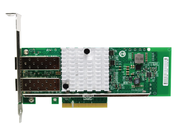
1 NET_PHY1000M_RTL8111GS IP核心芯片描述
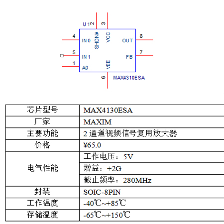
1.1 核心芯片1

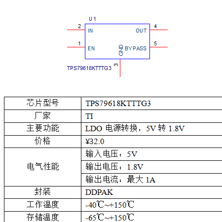
芯片型号 | RTL8111GS |
厂家 | REALTEK(瑞昱) |
主要功能 | PCIE X1信号转1000M以太网通信 |
价格 | ¥5.00 |
电气性能 | 接口电平:3.3V |
工作电流:≤70mA | |
PCI Express 速率:PCI Express 1.1 2.5Gbps | |
网口传输速率:1000M/100M/10M bps | |
IEEE:IEEE 802.3,IEEE 802.3u,IEEE 802.3ab,IEEE802.1Q VLAN,IEEE802.3az-2010 | |
工作温度 | 0°C~+70°C |
储存温度 | -55°C~+125°C |
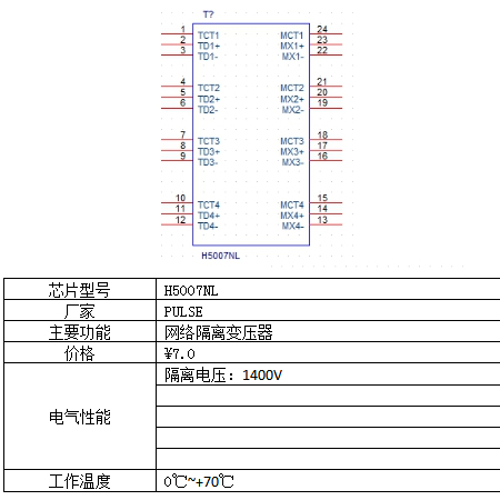
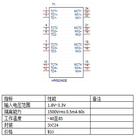
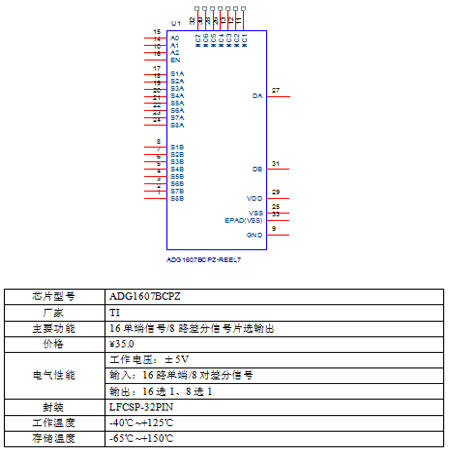
1.2 核心芯片2

芯片型号 | HR682480 |
厂家 | HanRun |
主要功能 | 1000M以太网变压器 |
价格 | ¥4.80 |
电气性能 | 匝数比 1:1 |
隔离电压:1500V | |
工作温度 | -40°C~+85°C |
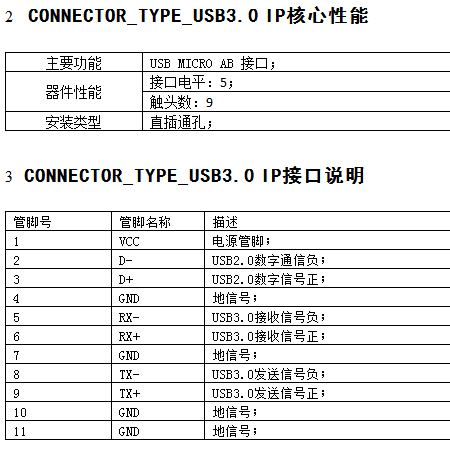
2 NET_PHY1000M_RTL8111GS IP核心性能
主要功能 | PCIE转1000M以太网通信,变压器隔离 |
电气性能 | 主芯片工作电压:3.3V |
工作电流:≤70mA | |
PCIE 速率:PCI Express 1.1 2.5Gbps | |
以太网速率:1000M/100M/10M bps | |
隔离电压:1500VDC | |
系统工作温度 | 0°C~+70°C |
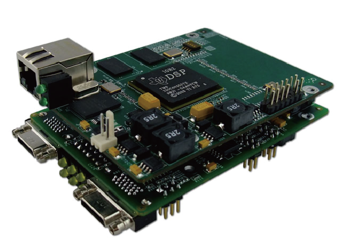
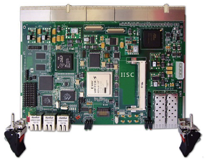
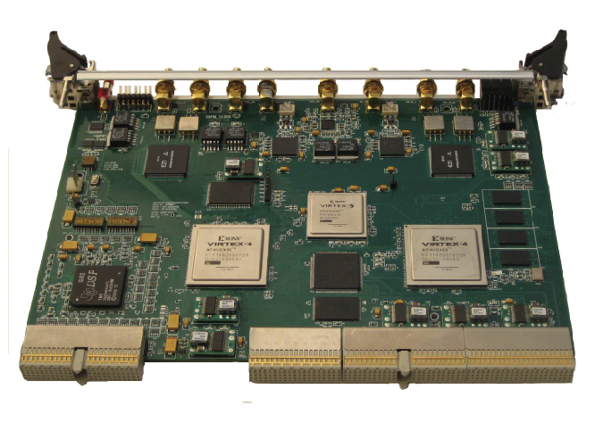
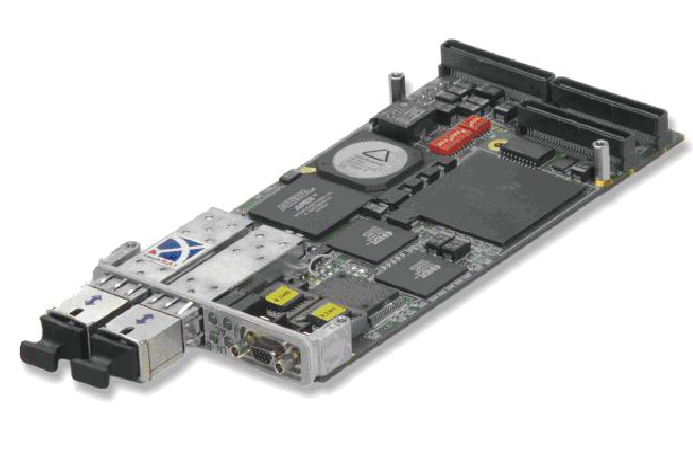
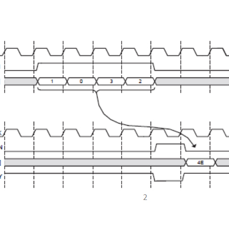
3 NET_PHY1000M_RTL8111GS IP应用
3.1 IP原理图示意
见原理图
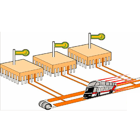
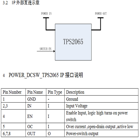
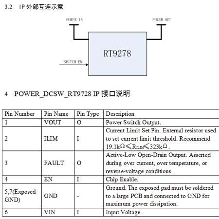
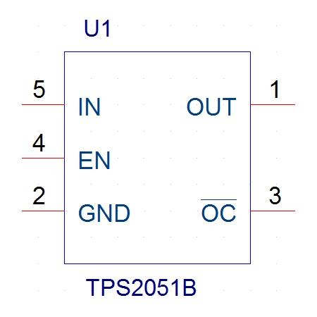
3.2 IP外部互连示意

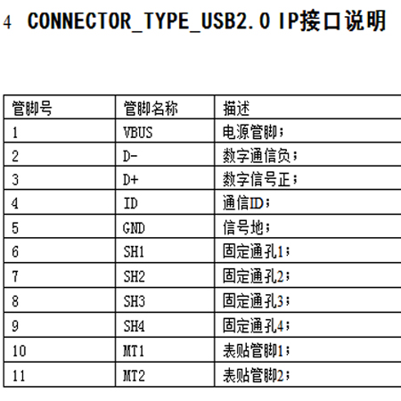
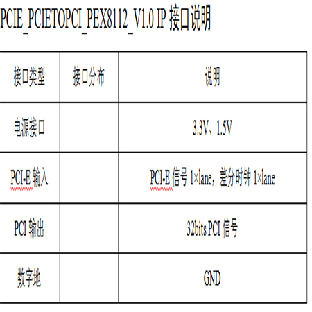
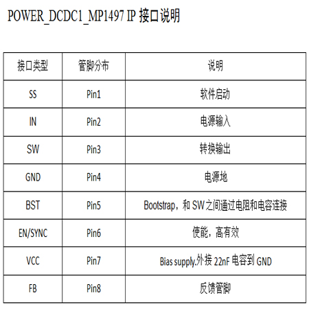
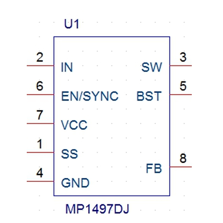
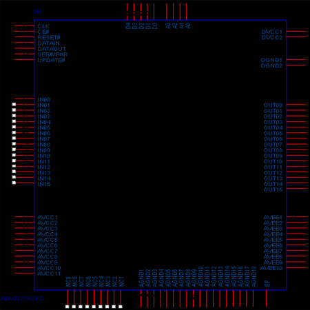
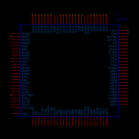
4 NET_PHY1000M_RTL8111GS IP接口说明
说明:
I:Input S/TS:Sustained Tri-State
O:Output O/D:Open Drain
T/S:Tri-State Bi-Directional Input/Output Pin P:Power
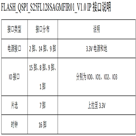
4.1 电源和地
Symbol | Type | Pin No | Desc |
AVDD10 | P | 3,8,30 | Analog 1.0V Power Supply |
DVDD10 | P | 22 | 1.0V Power Supply |
AVDD33 | P | 11,32 | 3.3V Power Supply |
GND | P | 33 | Ground(exposed Pad) |
4.2电源管理
Symbol | Type | Pin No | Desc |
LANWAKEB | O/D | 21 | Power Management Event:Open drain,active low. |
ISOLATEB | I | 20 | Isolate Pin:Active low. |
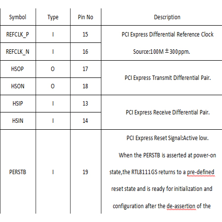
4.3 PCI Express 接口
Symbol | Type | Pin No | Desc |
REFCLK_P | I | 15 | PCI Express Differential Reference Clock Source:100M±300ppm. |
REFCLK_N | I | 16 | |
HSOP | O | 17 | PCI Express Transmit Differential Pair. |
HSON | O | 18 | |
HSIP | I | 13 | PCI Express Receive Differential Pair. |
HSIN | I | 14 | |
PERSTB | I | 19 | PCI Express Reset Signal:Active low. |
CLKREQB | O/D | 12 | Reference Clock Request Signal. |
4.4以太网信号接口
Symbol | Type | Pin No | Desc |
MDIP0 | IO | 1 | In MDI mode,this is the first pair in 1000Base-T,i.e,the BI_DA+/-pair,and is the transmit pair in 10Base-T and 100Base-TX. |
MDIN0 | IO | 2 | |
MDIP1 | IO | 4 | In MDI mode,this is the second pair in 1000Base-T,i.e,the BI_DA+/-pair,and is the transmit pair in 10Base-T and 100Base-TX. |
MDIN1 | IO | 5 | |
MDIP2 | IO | 6 | In MDI mode,this is the third pair in 1000Base-T,i.e,the BI_DA+/-pair. |
MDIN2 | IO | 7 | |
MDIP3 | IO | 9 | In MDI mode,this is the fourth pair in 1000Base-T,i.e,the BI_DA+/-pair. |
MDIN3 | IO | 10 |
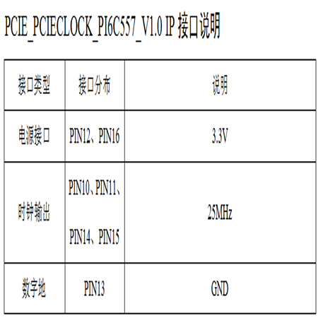
4.5 Clock
Symbol | Type | Pin No | Desc |
CKXTAL1 | I | 28 | Input of 25MHz or 48MHz Clock Reference. |
CKXTAL2 | IO | 29 | Input of External Clock Reference. |
4.6 Regulator and Reference
Symbol | Type | Pin No | Desc |
REGOUT | O | 24 | RTL8111GS:Switching Regulator 1.0V Output |
VDDREG | P | 23 | Digital 3.3V Power Supply for Switching Regulator. |
RSET | I | 31 | Reference External resistor reference. |
4.7 LEDs
Symbol | Type | Pin No | Desc |
LED0 | O | 27 | On only in 10M mode,with bl |
LED1/GPO | O | 26 | On only in 100M mode,with bl |
LED2 | O | 25 | On only in 1000M mode,with bl |
4.8 GPO Pin
Symbol | Type | Pin No | Desc |
GPO/LED1 | I/O | 26 | General Purpose Input/Output Pin. |
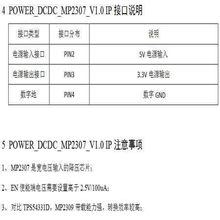
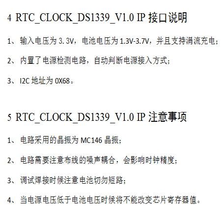
5 NET_PHY1000M_RTL8111GS IP注意事项
1、PCI Express 信号在PCB中走线时注意控制差分阻抗;
2、REGOUT信号是DCDC电路,尤其注意和RTL8111G芯片的区分,DCDC电路的电感之前不需要增加滤波电容;
3、以太网接口电路中,防静电处理使用高压电容即可,在PCB中注意布局和铺铜设计;
好评率:100%
好评数量:0个
工作速度:5分
工作质量:5分
工作态度:5分

暂无评价
CPU/GPU ¥12000.00
CPU/GPU ¥25000.00
CPU/GPU ¥10000.00
CPU/GPU ¥30000.00
CPU/GPU ¥10000.00
CPU/GPU ¥15000.00
CPU/GPU ¥10000.00
CPU/GPU ¥10000.00
其他 ¥5000.00

其他 ¥5000.00
其他 ¥10000.00
其他 ¥10000.00
其他 ¥10000.00
其他 ¥10000.00
其他 ¥10000.00

其他 ¥10000.00
FPGA电路 ¥10000.00
DSP电路 ¥10000.00
DSP电路 ¥10000.00
DSP电路 ¥10000.00
DSP电路 ¥10000.00
DSP电路 ¥10000.00
DSP电路 ¥10000.00
DSP电路 ¥10000.00
DSP电路 ¥10000.00
DSP电路 ¥10000.00
DSP电路 ¥10000.00
CPU/GPU ¥10000.00
FPGA电路 ¥10000.00
DSP电路 ¥10000.00
DSP电路 ¥10000.00
FPGA电路 ¥10000.00
DSP电路 ¥10000.00
CPU/GPU ¥10000.00
DSP电路 ¥10000.00
DSP电路 ¥10000.00
DSP电路 ¥10000.00
DSP电路 ¥10000.00
DSP电路 ¥10000.00
CPU/GPU ¥10000.00

FPGA电路 ¥10000.00
FPGA电路 ¥10000.00
模拟电路 ¥10000.00
模拟电路 ¥5000.00
模拟电路 ¥5000.00

模拟电路 ¥5000.00
模拟电路 ¥10000.00
模拟电路 ¥10000.00
DSP电路 ¥10000.00
DSP电路 ¥10000.00

DSP电路 ¥10000.00
FPGA电路 ¥10000.00

DSP电路 ¥10000.00

DSP电路 ¥10000.00
DSP电路 ¥10000.00
DSP电路 ¥10000.00
CPU/GPU ¥20000.00
CPU/GPU ¥20000.00
CPU/GPU ¥20000.00
CPU/GPU ¥20000.00
CPU/GPU ¥15000.00
CPU/GPU ¥20000.00
CPU/GPU ¥18000.00
CPU/GPU ¥20000.00
其他 ¥10000.00
其他 ¥6000.00
其他 ¥2000.00
其他 ¥3000.00
其他 ¥12000.00
其他 ¥8000.00
FPGA电路 ¥5000.00

MCU电路 ¥4800.00
嵌入式 ¥50000.00

嵌入式 ¥50000.00

嵌入式 ¥50000.00
嵌入式 ¥50000.00

嵌入式 ¥50000.00
嵌入式 ¥50000.00

嵌入式 ¥50000.00

嵌入式 ¥50000.00
嵌入式 ¥50000.00

嵌入式 ¥50000.00

嵌入式 ¥50000.00
嵌入式 ¥50000.00
嵌入式 ¥50000.00
嵌入式 ¥50000.00

嵌入式 ¥50000.00

嵌入式 ¥50000.00
嵌入式 ¥50000.00
嵌入式 ¥50000.00

嵌入式 ¥50000.00
嵌入式 ¥50000.00
嵌入式 ¥50000.00

嵌入式 ¥50000.00
嵌入式 ¥50000.00
嵌入式 ¥50000.00

嵌入式 ¥50000.00
嵌入式 ¥50000.00
嵌入式 ¥50000.00
嵌入式 ¥50000.00
嵌入式 ¥50000.00
嵌入式 ¥50000.00
嵌入式 ¥50000.00
嵌入式 ¥50000.00

嵌入式 ¥50000.00

嵌入式 ¥50000.00
嵌入式 ¥50000.00
其他 ¥50000.00
其他 ¥50000.00
其他 ¥50000.00
其他 ¥50000.00
其他 ¥50000.00
MCU电路 ¥50000.00
MCU电路 ¥50000.00
其他 ¥50000.00
其他 ¥50000.00
其他 ¥50000.00
其他 ¥50000.00
其他 ¥50000.00
其他 ¥50000.00
其他 ¥50000.00
其他 ¥50000.00
其他 ¥50000.00
其他 ¥50000.00
其他 ¥50000.00
其他 ¥50000.00
其他 ¥50000.00
其他 ¥50000.00
其他 ¥50000.00

其他 ¥50000.00
其他 ¥50000.00
其他 ¥50000.00
其他 ¥50000.00
其他 ¥50000.00
其他 ¥50000.00
其他 ¥50000.00
其他 ¥50000.00
其他 ¥50000.00

其他 ¥50000.00
其他 ¥50000.00
其他 ¥50000.00
其他 ¥50000.00
其他 ¥50000.00
其他 ¥50000.00
其他 ¥50000.00
其他 ¥50000.00
其他 ¥50000.00
其他 ¥50000.00
其他 ¥50000.00
其他 ¥50000.00
其他 ¥50000.00
其他 ¥50000.00
其他 ¥50000.00
其他 ¥50000.00
其他 ¥50000.00
其他 ¥50000.00
其他 ¥50000.00
其他 ¥50000.00
其他 ¥500000.00
其他 ¥50000.00
其他 ¥50000.00
其他 ¥50000.00
其他 ¥50000.00
其他 ¥50000.00
其他 ¥50000.00
其他 ¥50000.00
其他 ¥50000.00
其他 ¥50000.00
其他 ¥50000.00
其他 ¥50000.00
其他 ¥50000.00

其他 ¥50000.00
其他 ¥50000.00
其他 ¥50000.00
其他 ¥50000.00
其他 ¥50000.00
其他 ¥50000.00
其他 ¥50000.00
其他 ¥50000.00
其他 ¥50000.00
其他 ¥50000.00
其他 ¥50000.00
其他 ¥50000.00
其他 ¥50000.00
其他 ¥50000.00
其他 ¥50000.00
其他 ¥50000.00